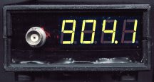
Easy to build high-quality PLL FM transmitter with typical output power of 5 W and no-tune design.
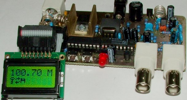
The transmitter includes RDS/SCA input and Audio/MPX input with optional preemphasis. It can be used with or without stereo encoder. Tuning over the FM band is provided by two buttons that control dual-speed PLL. The transmitter can work also without the LCD display.
Characteristics:

Following table shows typical output power at 90 MHz for different power supply voltages and output stage transistors.
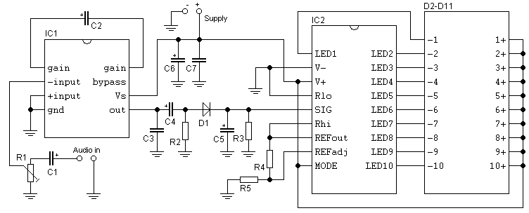
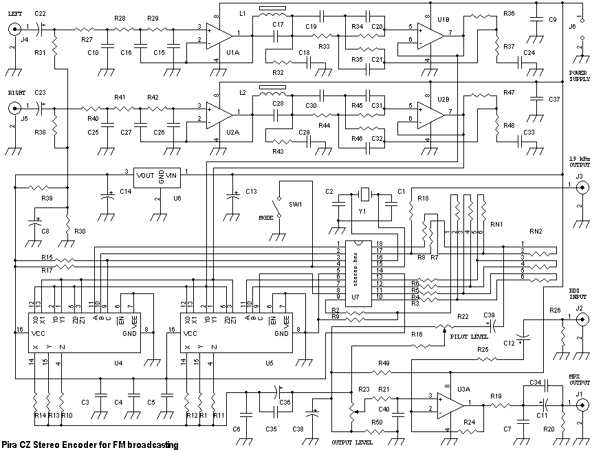
 Schematic diagram
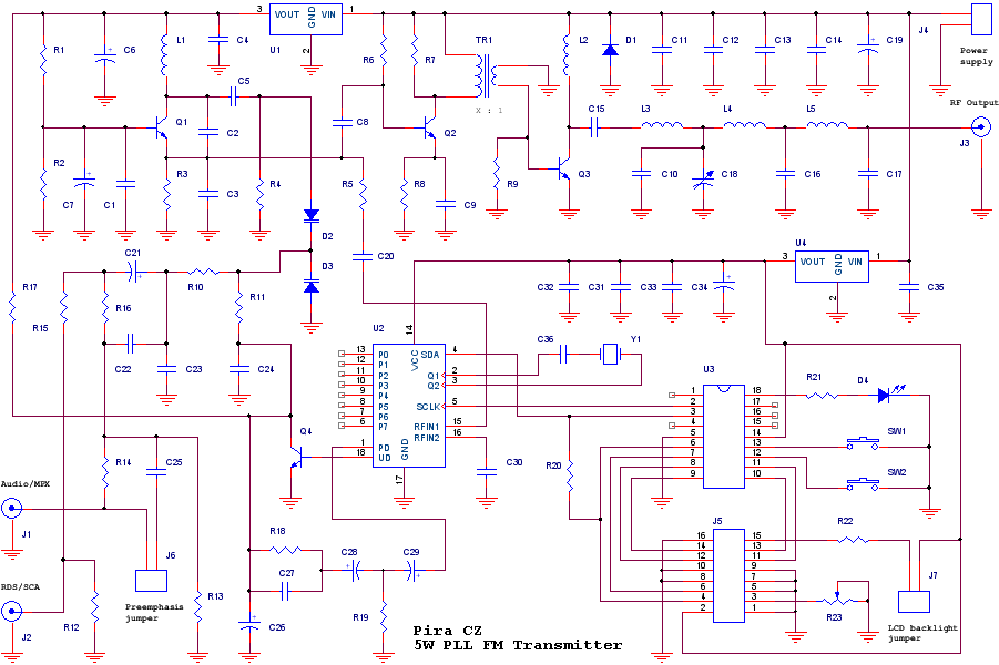
Part list
Q1 - BF240
Q2 - BFG135 (BFG235)
Q3 - 2SC1971 (2N3553) + heatsink
Q4 - BC547B
D1 - SB260 (1N5822, 1N581x)
D2, D3 - BBY40 (BBY31)
D4 - LED 5mm
U1 - 78L09
U2 - TSA5511 (TSA5512, SDA3202)
U3 - PIC16F627A (programmed)
U4 - 78L05
R1, R2, R11, R17, R20 - 10k
R3, R21 - 270R
R4, R15 - 33k
R5, R7, R12, R13, R16 - 680R
R6, R14 - 18k
R8 - 47R (33R if Q2 is BFG235)
R9 - 18R
R10 - 4k7
R18 - 3k3
R19 - 100k smd 1206
R22 - 91R
R23 - trimmer 5k mini
C1, C4, C9, C12, C13, C14, C15, C30, C31, C32, C33, C35 - 10n smd 1206 (C)
C2, C17, C20 - 15p (C)
C3 - 10p (C) (15p if the PCB is single-sided)
C5 - 1n (C)
C6, C28, C29, C34 - 100u/10V (E)
C7, C26 - 10u/35V (E)
C8 - 22p (C)
C10 - 47p (C) (33p if Q3 is 2N3553)
C11, C27 - 100n (C)
C16, C36 - 33p (C)
C18 - trimmer 50p
C19 - 470u/16V (E)
C21 - 4u7/50V (E)
C22 - 330p (C)
C23, C24 - 47p (C)
C25 - 3n3 (P)
L1 - 3.5 turns on 7 mm diameter
L2 - 1uH/815mA choke, or about 10 turns of thin wire on mini ferrite core
L3 - 2.5 turns on 6 mm diameter (4.5 turns if Q3 is 2N3553)
L4, L5 - 3.5 turns on 6 mm diameter
Y1 - crystal 6.4 MHz or 3.2 MHz
TR1 - rf ferrite transformer 2:1 (3:1 if Q3 is 2N3553), see text
SW1, SW2 - button mini
J1, J2, J3 - BNC connector 90 deg.
J4 - power supply connector
J5 - HD44780 LCD standard connector, 2x8 or 2x16 characters
J6, J7 - jumper
Additional information
For 0.05 MHz step tuning a 3.2 MHz crystal is required. In other case a 6.4 MHz crystal will make good work (step tuning 0.1 MHz).
Wind all coils (except the L2) by a 0.8 mm wire.
The Y1 package must be tied to ground!
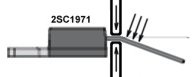
Make sure the Q3 terminals are as short as possible (about 2-3 mm above board). The 2N3553 case/heatsink can't be tied to ground!
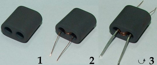
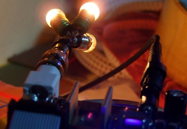
To make the TR1 transformer, use specified number of turns on primary side and one turn on secondary side. The secondary wire should be quite thick but the primary can be as thin as you want. Wind on a 2-hole ferrite (material 61 or N1). The picture explains it all:
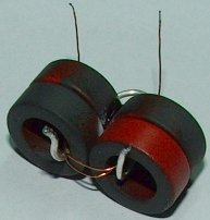
Alternatively use two ordinary ferrite beads placed side-by-side, something like on the picture:
Be careful when forming the 2SC1971 terminals - you may corrupt its internal structure! Or leave the terminals straight and use another suitable heatsink.
Control software for U3
The software for U3 is provided for download here: plltsa.zip (version 1.3). Please read included license text first.
Suitable free PIC programmer is for example here: http://www.members.aon.at/electronics/pic/picpgm/. Actually Pira CZ does not provide the PIC programming or complete kit sale for this device.
Software modifications included: pll64.hex - 6.4 MHz crystal, pll32.hex - 3.2 MHz crystal, pll.asm - for any changes.
Fuses: WDT: Enabled, OSC: INTRC-I/O, MCLRE: I/O.
Use the buttons to set the frequency. After a few seconds of idle the frequency is tuned and stored to EEPROM (icon of diskette). Finally the buttons are locked (icon of key) to avoid unwanted frequency changes. Unlock by pressing any button for a longer time.
The display and LED indicate PLL in-lock state. This state is also provided at pin 1 of U3. It can be used for control of additional power amplifier. When in-lock state is indicated, the PLL is switched to low speed for maximally flat low audio frequencies response.
Placing in operation
 After complete parts placement:
Check that there are no shorts bridging adjacent tracks or pads.
Check electrolytic capacitors polarity and semiconductor parts orientation.
Make any duty load and connect it temporarily to the antenna connector. Use for example 2 or 3 bulbs (24V/170mA or 24V/3W) in parallel (see the picture).
Start with smaller power supply voltage, for example 9 V. The bulbs should glow a little. Then it's OK and you may increase the power supply voltage to 12 V. Adjust C18 to max. output power. Adjust right LCD contrast by R23.
Now the L1 coil must be adjusted by stretching or compressing the turns. It affect frequency position of the band, which is the PLL able to tune.
Tune to 107.9 MHz using the buttons.
Measure tuning voltage at Q4 collector. Set the tuning voltage to 8.0 V by adjusting the L1.
Then you are done.
Now tune to 105 MHz and adjust C18 to max. power finally. At this point use about 10 meters of coaxial cable between the transmitter and the duty load!
If you have a problem with stability/spurious oscillations (very improbably if you used standard components and procedures), you may:
decrease R7 or R9 value
increase R8 value
decrease power supply voltage
use another material for TR1
If you want to change the output power, you may do it by changing the R8 value. Don't use smaller values than mentioned in part list!
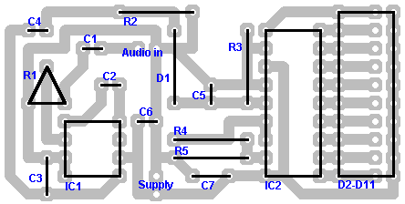
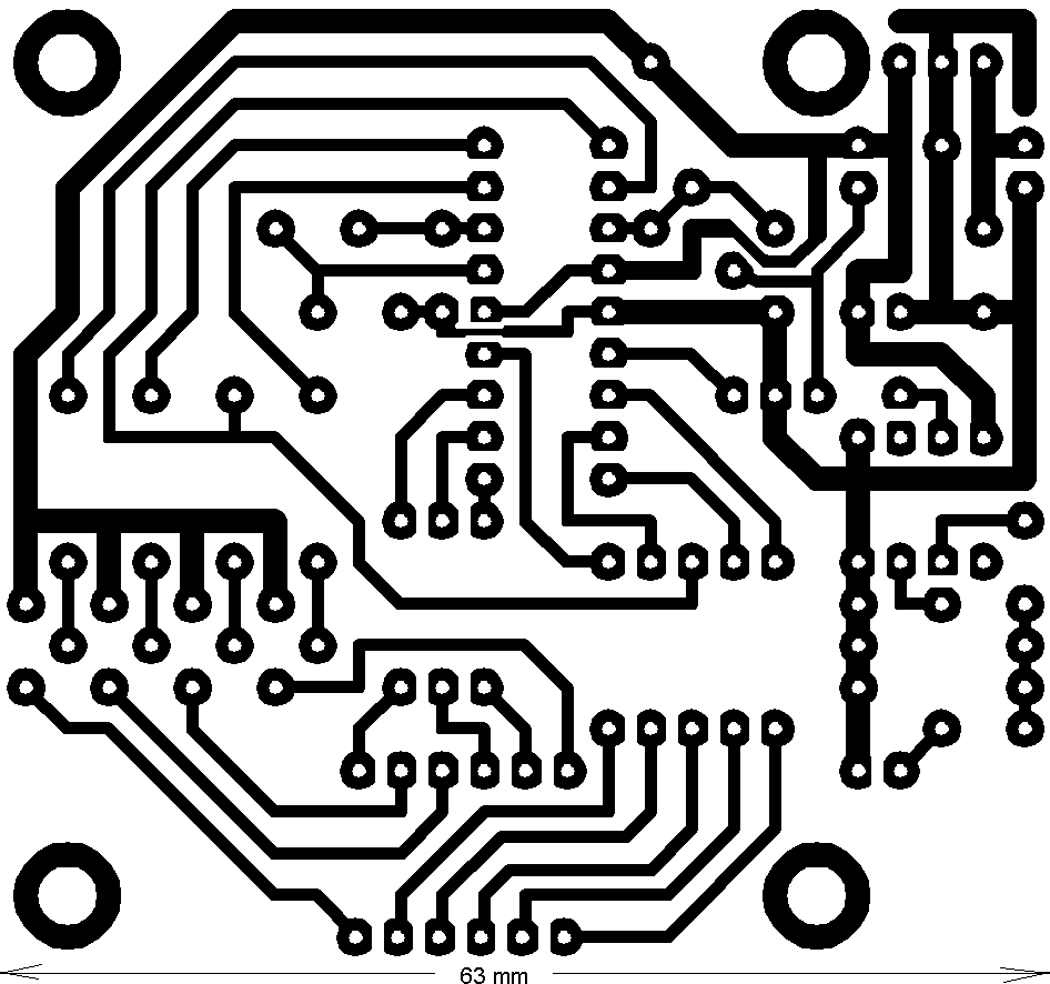
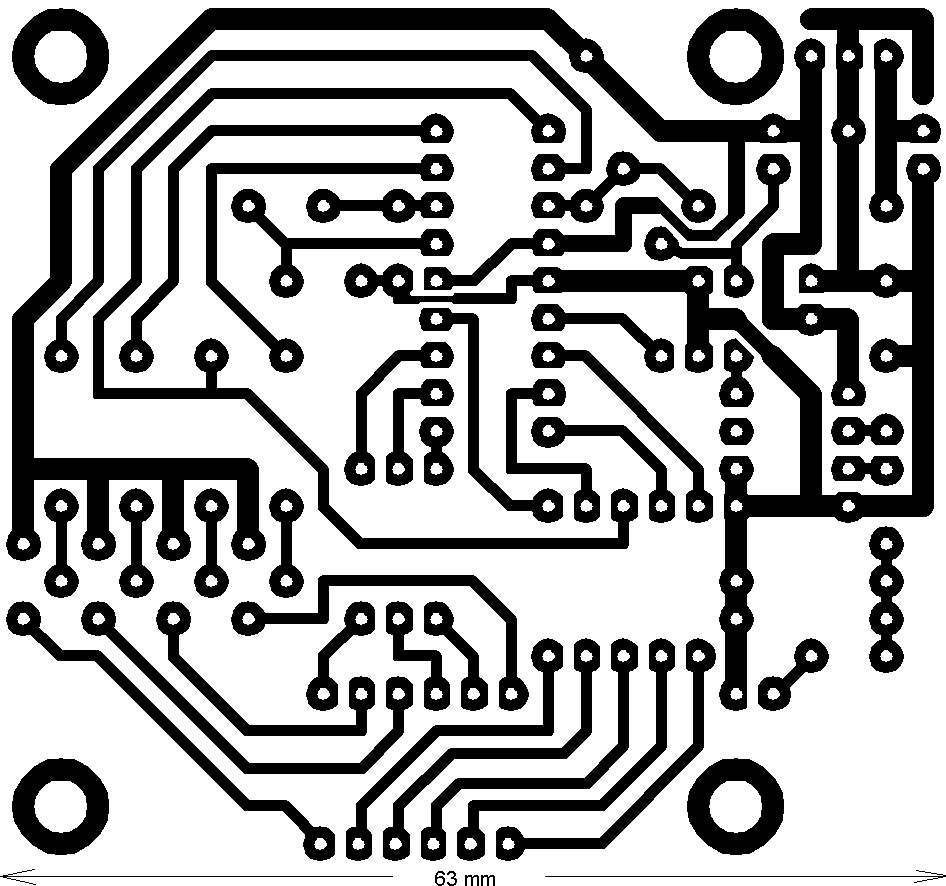
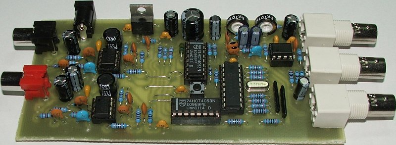
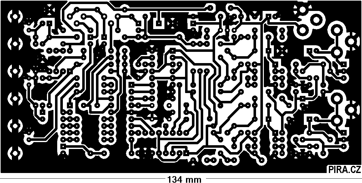
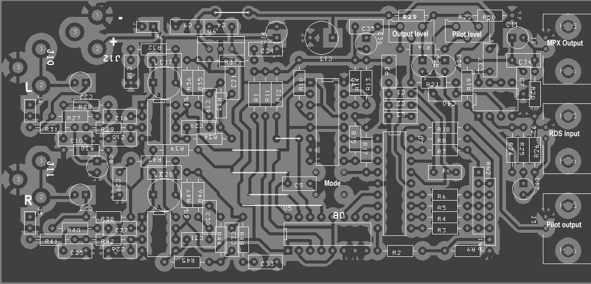
PCB
You may choose between single-sided PCB (only bottom layer) and double-sided PCB (+ ground layer on the top). The difference is in output power. The double-sided PCB gives higher output power (this fact is not so interesting in rf issue).
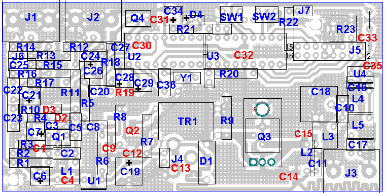
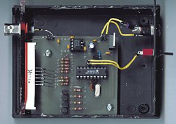
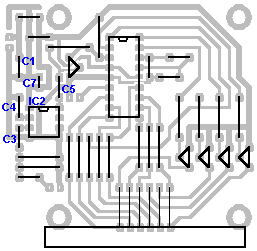
Parts placement.
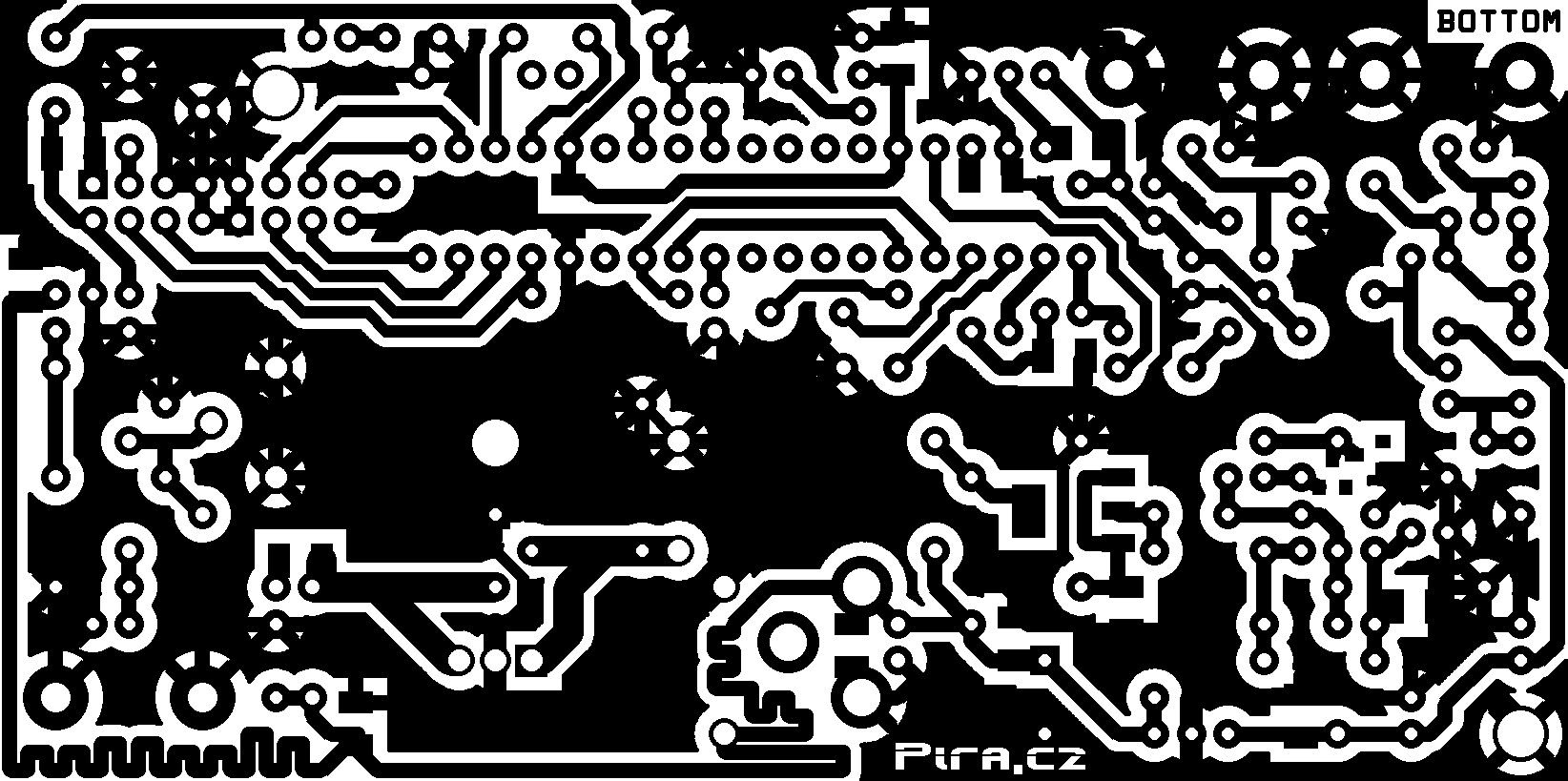
Bottom side.
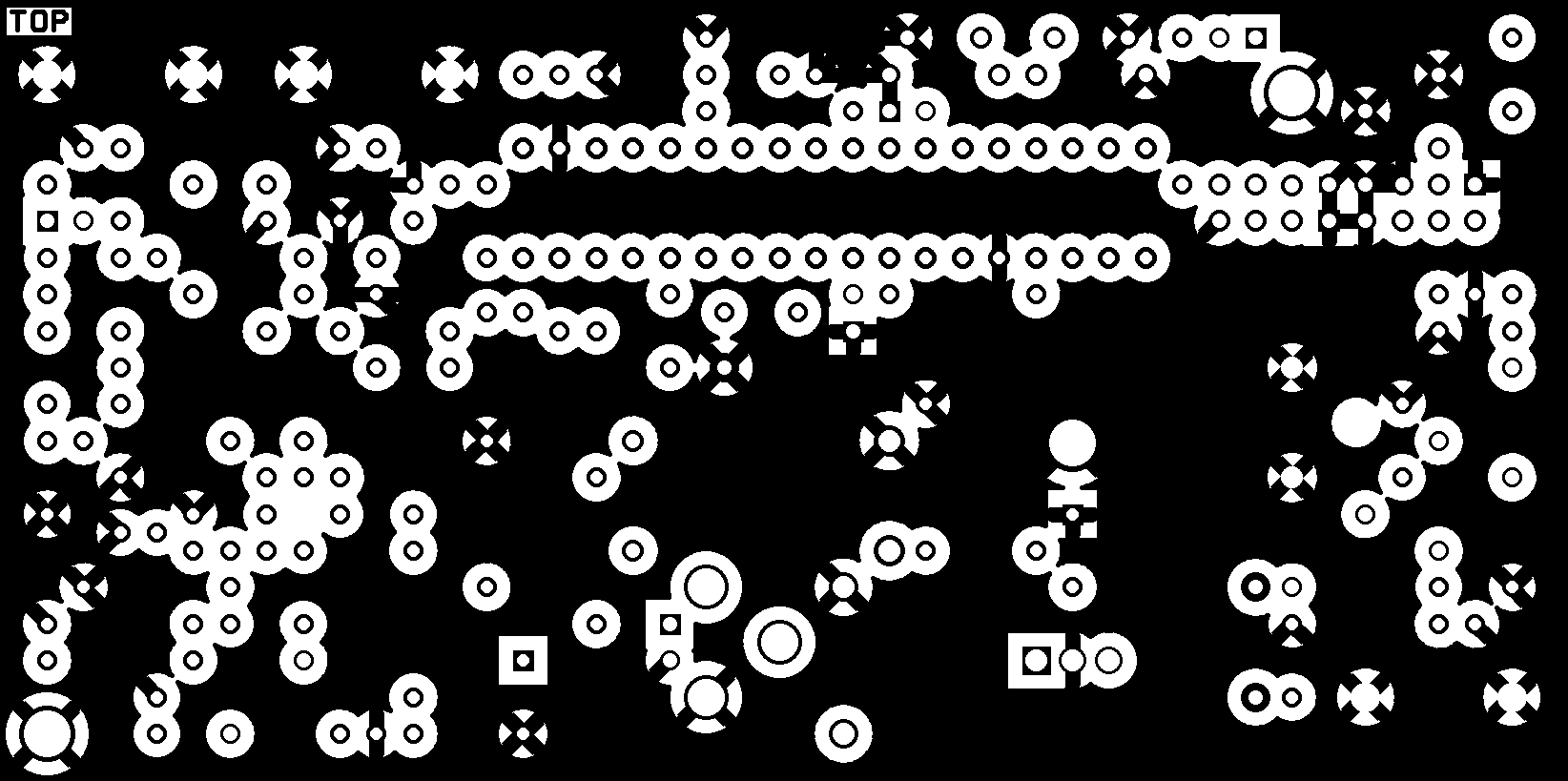
Top side (optional).
The board dimensions are 109 x 54 mm. If double-sided PCB is used, don't forget to solder ground pins of key parts also from top side (mainly Q3, TR1, U1, D1, U4, SW1, SW2, R3, R8, C11).
You may buy the printed circuit board or fully assembled transmitters in the shop.
| Drill chart |
| Diameter | Quantity |
| 0.8 mm | 151 |
| 1.0 mm | 50 |
| 1.5 mm | 10 |
| 2.0 mm | 6 |
| 2.5 mm | 3 |
| 3.2 mm | 3 |
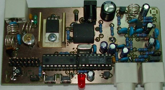
Double-sided PCB, 2SC1971.
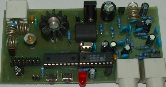
Single-sided PCB, 2N3553.
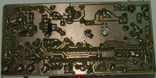
Bottom side with smd parts.
Source : http://pira.cz/entx4.htm
Read More..

 Features
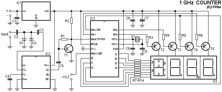
 IC3 program download:
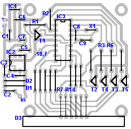


